WINSOK sgt mosfet new products on-line, SGT technology is the future of mosfet?
 2020/9/21 15:44:41
Recently, the resistance of MOSFET can be further reduced by reducing the electric field of the MOSFET. At present, winsok's new generation of low and medium voltage power MOSFETs widely use this technology, such as: WSD40120DN56G,WSD14N10DNG,WSF15N10G,WSF45N10G and other models with "G" suffix. In fact, the magic MOSFET technology is Sgt technology.
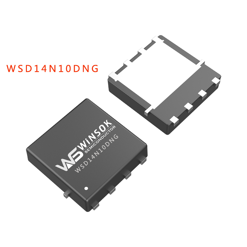
WINSOK SGT MOSFET——WSD14N10DNG《This drawing is for reference only, and is mainly in kind》
In recent years, as a new technology of MOSFET, more and more manufacturers pay attention to Sgt process and invest a lot of financial resources and resources. From the perspective of the whole industry, in the field of medium and low voltage MOSFETs, Sgt process technology is also the cutting-edge power device technology in the industry. Among them, the best companies and manufacturers are Infineon and other international power semiconductor plants.
Next, a brief introduction to the SGT process MOSFET and its advantages.
Although IGBT is very popular now, compared with MOSFET, it is also a high-end power device, but MOSFET still occupies a huge market share in the majority of medium and low-voltage applications, whether it is consumer electronics, household appliances, or embedded systems and industrial fields. Therefore, many companies and manufacturers at home and abroad continue to increase investment in corresponding new technology research and development, such as winsok.
MOSFET is characterized by high input impedance, low control power, fast switching speed and low switching loss. It is widely used in high frequency, medium and small power applications (voltage below 600V), especially in consumer electronics.
MOSFETs can be roughly divided into the following four categories: planar MOSFET; trench MOSFET, which is mainly used in low voltage (100V) field; Sgt process (shielded gate transistor) MOSFET, mainly used in low voltage (200V) field; sj-mosfet, namely superjunction MOSFET, is mainly used in high voltage (600V-800V) field.
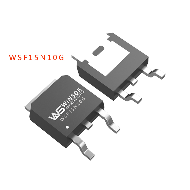
WINSOK SGT MOSFET——WSF15N10G
Compared with the common trench, Sgt process is simpler, lower switching loss, smaller junction capacitance, narrow Miller platform and low internal resistance. Specifically, the depth of Sgt is 3-5 times deeper than that of conventional trench process, and a polysilicon electrode is added under the gate electrode, that is, shielding electrode or coupling electrode. The shield electrode is connected with the source electrode, which realizes the function of shielding gate and drift area, reduces Miller capacitance, speeds up the switching speed of the device, realizes the charge coupling effect, reduces the critical electric field intensity in the drift region, reduces the on resistance of the device and reduces the switching loss. Compared with conventional trench MOSFET, the internal resistance of Sgt process MOSFET is more than 2 times lower.
The chip area of MOSFET is reduced by more than 40% at the same power consumption compared with ordinary trench MOSFET by reducing parasitic capacitance and on resistance of FET by Sgt technology. The unique device structure and mask layout design of Sgt process technology improve the product durability and reduce the chip area, while its unique process design reduces the process steps and the number of masks, so as to reduce the production cost of MOSFET, and make the MOSFET products highly cost-effective and more competitive.
Compared with conventional trench MOSFET and planar MOSFET, the power density of the MOSFET fabricated by Sgt technology has a great advantage. Due to the deep groove depth of the SGT MOSFET, more silicon volume can be used to absorb the energy of EAS, so Sgt process can do better in avalanche and withstand avalanche breakdown and surge current.
After 2010, with the rapid charging of mobile phones, electric vehicles, brushless motors and lithium batteries, the demand for medium voltage MOSFETs is increasing, and the medium voltage power devices are booming. So far, the market scale of medium voltage power devices is larger than that of high-voltage power devices, second only to low-voltage power devices. The SGT process MOSFET is the representative of medium voltage power devices.
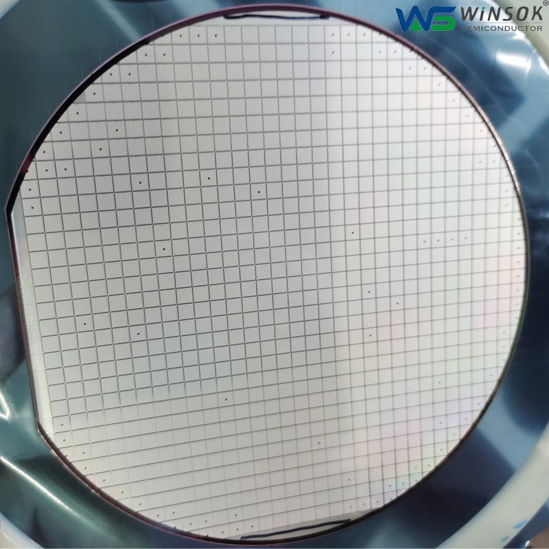
MOSFET 6 inch wafer
Technical iteration
Some people in the industry claim that the SGT MOSFET will not be replaced by other products in five years, and there will be some technical iterations in the future. Iteration is the continuous progress and effective matching of packaging technology and chip technology.
In addition to the R & D and iteration of chip technology, the progress of packaging technology will play an important role in Sgt process, such as 150V and 200V MOSFET. For example, the internal resistance of 150V MOSFET packaged with dfn5x6 can be less than 8 mΩ, and that of 200V MOSFET packaged with TO-220 can be less than 9 mΩ.
In addition to the external packaging, based on the change of the demand for MOSFET in electronic manufacturing, the internal packaging technology has been constantly improved, mainly reflected in three aspects: improving the interconnection technology inside the package, adding drain heat sink plate and changing the direction of heat conduction. These are very important for the development of Sgt technology.
TO, D-PAK, SOT, SOP and so on adopt soldered wire type internal interconnection packaging technology. When CPU or GPU power supply develops to the era of low voltage and high current, SO-8 package with soldered wire is limited by package resistance, package inductance, PN junction to PCB and shell thermal resistance.

The future of Sgt MOSFET
These four limitations have great influence on the electrical and thermal properties of MOSFET. With the increase of current density, MOSFET manufacturers have improved the solder wire interconnection form synchronously when adopting SO-8 size specification, replacing the solder wire with metal tape or metal splint, so as to reduce the package resistance, inductance and thermal resistance.
Generally speaking, with the development of electronic manufacturing industry towards ultra-thin, miniaturization, low voltage and high current, the shape and internal packaging structure of MOSFET will also change to better meet the development needs of manufacturing industry. In addition, in order to reduce the selection threshold of electronic manufacturers, the development trend of MOSFET towards modularization and system level packaging will become more and more obvious, and the products will develop harmoniously from the aspects of performance and cost.
As an important reference factor for the selection of Sgt MOSFET, different electronic products have different electrical requirements, and different installation environment also needs the matching size specification.
Moreover, if you want to innovate, you must have the ability to customize Sgt process products. Different Sgt technology and manufacturing process are needed in different application fields. Different chip manufacturers have different process platforms, equipment and corresponding Sgt process products. The epitaxial layer of raw materials is also different, which needs to be customized.
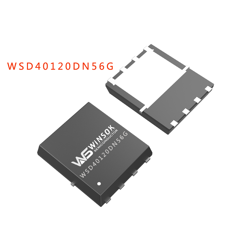
WINSOK SGT MOSFET——WSD40120DN56G
Market trends
From the application level, Chinese enterprises have been in the field of thyristor and MOSFET with large market space, scattered downstream applications and low entry threshold. At present, Chinese enterprises have made breakthroughs in the fields of consumer electronics, white household appliances, industrial control and new energy, but few MOSFET enterprises have really entered the field of high-end automobile.
Yole D é development, a French market research organization, has predicted that MOSFETs will have three obvious structural changes in the next five years: first, trench MOSFET will move down from the middle end to the low end, replacing some of the low-end market of planar MOSFET; second, advanced trend MOSFET such as Sgt technology will move down to the middle end, replacing trench MOSFET is in the middle end market of low voltage field. Third, wide bandgap MOSFETs such as SiC and Gan will occupy the high-end market.
Driven by this market development trend, the development strategy and planning of the enterprise must be followed up in time, and it is necessary to move towards a higher level, and shift the power device capacity from low-end MOSFET to high-end Sgt process and sj-mosfet. Through adjustment, we should try our best to stay away from the Red Sea market of ordinary MOSFET with fierce competition and low price, just like micro master, focusing on the middle and high-end MOS tube market.
With the development of 5g, AI, ev (electric vehicle) and other application markets, the demand for high-end MOSFET, IGBT, SiC and Gan is also growing rapidly. Many power semiconductor manufacturers begin to lay out the SGT process MOSFET with high power density and low internal resistance. The demand for Sgt process MOSFETs in both existing and emerging markets will continue to grow.
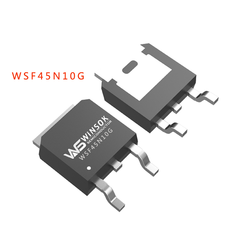
WINSOK SGT MOSFET——WSF45N10G
At present, foreign brands have gradually withdrawn from China's low-end MOSFET market, mainly due to the competitive pressure of domestic brands. Compared with previous years, China's power device manufacturers have made great progress in terms of scale and performance. In addition, with the advantages of cost, it is difficult for foreign brands to compete with domestic brands in the middle and low-end MOSFET market.
Nowadays, with the gradual decline of high-end MOSFETs in the market, and the development of high-end products by high-power semiconductor manufacturers, Sgt MOSFET has a broader development space, and WINSOK is precisely for this reason.
Back
- Previous:None
- Next:Marking adjustment information
